

Views: 0 Author: Site Editor Publish Time: 2026-10-24 Origin: Site


Selecting the incorrect silicone rubber profile can cause catastrophic electrostatic discharge (ESD) damage in sensitive electronics. It can also lead to dangerous dielectric breakdowns in high-voltage environments. We constantly face this high-stakes engineering challenge when designing modern components. Standard silicone is inherently non-conductive and acts as an excellent barrier against electrical currents. However, specialized compounding fundamentally alters its electrical properties. Manufacturers must manipulate these materials to meet strict industrial compliance standards. You must choose correctly to avoid severe safety risks and operational failures in your end products.
Our article provides a clear technical evaluation framework for your engineering team. We will help you decide between antistatic vs insulating silicone rubber formulations based on objective metrics. You will learn how to assess volume resistivity targets and navigate frustrating mechanical trade-offs. We also cover the practical processing realities you will face on the production floor. By understanding these core differences, you can design safer, more reliable components for any electrical application.
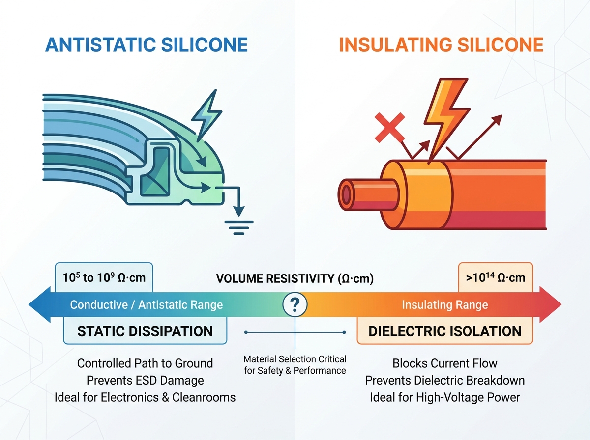
Standard electrical insulating silicone rubber boasts a volume resistivity exceeding 10¹⁴ Ω·cm, ideal for isolating high-voltage currents and preventing electrical tracking.
Antistatic formulations typically range from 10⁵ to 10⁹ Ω·cm, safely bleeding off static charges before they can spark or damage components.
Compounding standard silicone with additives like carbon black or specialized antistatic fumed silicone rubber alters not just conductivity, but also mechanical attributes like tear strength and color availability.
Material selection must account for specific processing behaviors, as antistatic fillers can impact mold flow, shrinkage rates, and curing times compared to unmodified insulating silicones.
Engineers must define clear success criteria before evaluating any polymer. You must first clarify the primary electrical function of your specific component. Is your main goal to prevent a massive electrical current from passing between two conductive points? We call this objective dielectric isolation. Alternatively, do you need to provide a controlled, steady path to ground for rogue static buildup? We define this as static dissipation. These two engineering goals demand entirely different material behaviors.
Misapplication carries severe and expensive consequences. Imagine installing an insulating silicone gasket in an ESD-sensitive semiconductor cleanroom. The friction generates a massive static charge on the surface. The material then attracts microscopic particulates, destroying cleanroom compliance. Worse, a sudden discharge could instantly fry thousands of sensitive integrated circuits (ICs). Now, consider the reverse scenario. Imagine using an antistatic silicone boot in a high-voltage power distribution network. The conductive properties allow current to leak out. You will experience immediate short circuits, severe thermal tracking, and potential electrical fires.
We use an objective evaluation metric to prevent these disasters. You must strictly utilize the surface and volume resistivity scale. This spectrum categorizes material performance objectively:
Conductive: Less than 10⁴ Ω.
Antistatic (Dissipative): 10⁵ to 10⁹ Ω.
Insulating: Greater than 10¹¹ Ω.
You must map your component requirements directly to this resistance spectrum. Doing so removes harmful guesswork and aligns your procurement team with reality.
We must examine the underlying chemistry to understand how these materials perform under stress. An inherent Si-O (siloxane) backbone structure defines standard silicone. This incredibly strong chemical bond provides natural dielectric strength. It resists the flow of electrical current naturally. You need minimal filler modification for standard electrical insulating applications. The unmodified base polymer does most of the heavy lifting against high voltages.
Antistatic variants require a much more aggressive compounding approach. Manufacturers must engineer the antistatic properties intentionally. They mix specific conductive additives directly into the raw silicone matrix. Traditional additives include fine carbon black, metallic powders, or even advanced carbon nanotubes. These fillers connect and create microscopic conductive networks within the cured rubber. They allow static charges to travel through the material safely and reach a ground point.
However, traditional carbon black has frustrating limitations. It completely turns the material opaque black. It can also shed tiny particles during mechanical flexing. To solve this, leading manufacturers now use a specialized antistatic fumed silicone rubber base. This modern base material maintains better optical clarity. It also preserves tear strength much better than old carbon-loaded mixtures. You achieve the required antistatic performance without suffering severe structural compromises.
You must understand the physical property trade-offs involved in compounding. Achieving a remarkably lower electrical resistivity often compromises other mechanical traits. Adding dense fillers reduces the overall elasticity of the final part. It often lowers the ultimate tensile strength. You will also notice a significant increase in Shore A hardness. The rubber becomes noticeably stiffer and harder to stretch. We recommend balancing your electrical targets against these physical realities during the prototyping phase.
Antistatic silicone serves critical protective roles in modern manufacturing environments. We deploy it primarily in pharmaceutical and semiconductor cleanrooms. It is absolutely essential for delicate electronic packaging seals and EMI/RFI shielding gaskets. You will also spot it on high-speed conveyor belts handling expensive microelectronics. These fast-moving environments cannot tolerate random static discharges.
We evaluate antistatic performance across two critical dimensions. First, we carefully measure the decay time. This laboratory metric shows how rapidly the material bleeds off an accumulated charge. A standard industry test measures the exact time it takes to drop a massive 1000V charge down to a safe 10V. Faster decay times translate to superior protection for sensitive components. Second, we verify environmental stability. The antistatic properties must remain permanent throughout the product lifecycle. They cannot rely on ambient room humidity to function properly. Cheap surface-applied anti-stat sprays simply wash off or evaporate. Compounded antistatic silicone guarantees permanent, humidity-independent protection.
Implementation Risks and Best Practices
You must watch out for the dreaded "sloughing" effect. Heavily loaded carbon-black silicones can shed fine conductive carbon dust during normal operation. This shedding causes devastating particulate contamination. It will instantly ruin ISO-certified cleanroom environments. We strongly recommend specifying modern fumed silica-based formulations to solve this.
Common Mistake: Specifying a highly conductive silicone (10⁴ Ω) when your application only requires basic static dissipation. This severe over-specification skyrockets material costs and ruins part elasticity.
Best Practice: Always demand rigorous cleanroom compatibility certificates. Ensure your selected material passes strict outgassing and particulate generation tests before authorizing mass production.
High-voltage utility applications demand extreme and uncompromising reliability. We rely heavily on premium electrical insulating silicone rubber to handle these immense loads. Primary industrial use cases include thick high-voltage cable jacketing and robust transformer potting compounds. You will also find it molded into automotive spark plug boots and massive utility-grade suspension insulators. These critical components must isolate lethal electrical currents efficiently.
We use rigorous performance evaluation dimensions for these insulators. First, we rigorously test dielectric strength. This metric measures the exact breakdown voltage (kV/mm) while under continuous, punishing electrical stress. The material must resist the high voltage without chemically failing. Second, we closely evaluate tracking and erosion resistance. High-voltage surface electrical discharges easily burn standard commodity plastics. They form permanent, conductive carbon tracks across the surface. Premium insulating silicone easily withstands these harsh discharges without forming any tracking paths. Finally, we assess long-term thermal stability. The insulating rubber must maintain its exceptional dielectric properties under extreme temperature swings. It routinely achieves impressive Class H insulation ratings, surviving continuous exposure up to 180°C.
Implementation Risks and Best Practices
You must prioritize absolutely void-free molding above all other manufacturing concerns. Trapped microscopic air is the ultimate enemy of high-voltage insulation. Air pockets trapped inside the silicone matrix act as dangerous failure points. They trigger localized corona discharges when exposed to high fields. These invisible discharges slowly erode the polymer from the inside out. They inevitably lead to catastrophic premature equipment failure.
Common Mistake: Ignoring proper mold venting designs. Poor tool venting traps air bubbles, instantly ruining the dielectric integrity of the finished part.
Best Practice: Utilize vacuum-assisted liquid injection molding for all critical insulators. This advanced process removes ambient air before the curing cycle even begins.
Material selection directly dictates the reality on your manufacturing floor. You must drastically adapt your processing techniques based on the chosen silicone profile. Curing mechanisms play a massive role in overall production success. We generally contrast high-purity platinum-cured systems against traditional peroxide-cured systems. Platinum curing provides higher purity, faster cycle times, and precise dimensional stability. However, adding antistatic fillers heavily complicates this chemistry. Certain conductive additives contain traces of sulfur or amines. These act as severe curing inhibitors. They can easily poison the delicate platinum catalyst if the compound is not formulated carefully.
Mold flow dynamics and shrinkage rates also change dramatically. Highly filled antistatic silicones exhibit much higher un-cured viscosity. They are significantly thicker and much harder to pump. You will need adjusted injection pressures to fill the tool. You might also require larger mold gate sizing to prevent severe sheer stress on the material. Furthermore, shrinkage rates differ widely between standard insulating rubbers and heavily modified antistatic rubbers. You cannot simply use an existing legacy mold. If you migrate a component design from an insulating to an antistatic rubber, you must modify your tooling. The final part will shrink differently during the post-cure oven phase.
Strict compliance and testing standards guide all these implementations. You must align your materials to relevant industry safety standards. We rely on ANSI/ESD S20.20 for designing static control environments. We heavily depend on ASTM D149 for measuring the exact dielectric breakdown voltage in insulating rubbers.
Table 1: Processing Comparison Summary
Processing Parameter |
Standard Insulating Silicone |
Antistatic Silicone (Filled) |
|---|---|---|
Viscosity & Flow Dynamics |
Low to moderate viscosity; effortlessly fills complex, intricate mold cavities. |
High viscosity; demands larger gates and significantly higher injection pressures. |
Post-Cure Shrinkage Rate |
Highly predictable (typically falls between 2% and 3%). |
Variable; heavy dense fillers often reduce the overall shrinkage percentage. |
Chemical Curing Risks |
Minimal risks observed with standard platinum or peroxide catalysts. |
Additives may strongly inhibit platinum catalysts; requires batch testing. |
Tooling Adjustments |
Accepts standard gate dimensions and basic atmospheric venting. |
Requires robust vacuum venting and hardened, reinforced tooling steel. |
Choosing the right material profile requires a highly systematic approach. We utilize a straightforward three-step decision framework. This structured process eliminates costly guesswork and fiercely protects your project timeline.
Identify the Specific Electrical Requirement. You must mandate precise resistivity targets immediately. Base these numerical targets on the official regulatory or safety standards of your specific industry. Do not guess or estimate. Verify exactly if you need >10¹⁴ Ω·cm for complete isolation or 10⁶ Ω·cm for controlled ESD dissipation.
Assess Mechanical and Aesthetic Needs. Evaluate the strict physical constraints of your design. If you require exact color-matching or visual transparency, you face immediate limits. Heavily carbon-loaded antistatic silicones are strictly opaque black. They are totally disqualified for clear applications. You must evaluate alternative, lighter conductive fillers if part aesthetics matter.
Prototype and Rigorously Test. Never skip physical hardware validation. We strongly recommend requesting cured material plaques directly from the compounder. Conduct your own in-house dielectric strength or surface resistance testing. You must meticulously verify these core metrics prior to cutting expensive steel production tooling.
By executing these specific steps, you mitigate severe technical risks very early. You ensure the final molded product meets both rigorous electrical demands and mechanical lifespan expectations.
The engineering choice between antistatic versus insulating silicone rubber is rarely ambiguous. It demands precise specification of resistivity tolerances long before production begins. You must lock in these critical numbers early in the initial design phase to prevent downstream failures.
Evaluating the secondary manufacturing impacts of these materials is crucial for success. Variables like tooling shrinkage, strict cleanroom compatibility, and chemical curing inhibitors actively dictate your production timeline. Managing these distinct variables separates a smooth, successful product rollout from extremely costly manufacturing delays.
We advise engineers to take proactive action immediately. Consult directly with your material compounder very early in the DFM (Design for Manufacturing) phase. Secure the exact material data sheets. Request physical sample batches and confidently validate your mathematical assumptions through rigorous real-world prototyping.
A: Yes, it is entirely possible. Manufacturers avoid traditional carbon black by using inherently dissipative polymers or specialized fumed silica additives. These advanced alternatives provide excellent static dissipation while allowing the rubber to remain translucent or be pigmented in custom colors.
A: Standard electrical insulating silicone rubber maintains a remarkably high volume resistivity. The standard threshold consistently exceeds >10¹⁴ Ω·cm. This massive resistance perfectly blocks the flow of electrical current, making it ideal for isolating high-voltage power components safely.
A: It depends heavily on the specific additive chosen. While the pure base silicone easily handles extreme high heat, certain organic antistatic additives may degrade rapidly at lower temperatures. You must mandate careful filler selection to maintain the expected thermal endurance.
A: You verify these properties using standard electrical testing equipment. Engineers rely on precise megohmmeters combined with surface resistivity meters. Utilizing specialized concentric ring probes ensures accurate, repeatable measurements across the surface of your molded component.


